CDR_BangBangPLLCDR : A bang-bang PLL based clock-and-data recovery unit (CDR)
A clock-and-data recovery unit (CDR) is a key component in high-speed wireline receivers that recovers an optimal clock to sample and detect an incoming data stream. In particular, a bang-bang PLL based CDR is a feedback system that adjusts the phase and frequency of the recovered clock produced by an oscillator based on the timing error information provided by a bang-bang phase detector.
This bang-bang PLL based CDR model basically describes a phase-locked loop (PLL) composed of an Alexander-type bang-bang phase detector, a digital loop filter, and a digitally-controlled oscillator (DCO). The bang-bang phase detector detects the timing error between the incoming data carried by the differential inputs inp and inn and the recovered clock clk and produces the signals up and dn expressing the polarity of the timing error, that is, whether the timing is early or late. The digital loop filter then processes this information and adjusts its 14-bit digital output dctrl, controlling the frequency and phase of the DCO output clock clk.
Ref: R.C. Walker, et al., “A Two-Chip 1.5-GBd Serial Link Interface,” IEEE Journal of Solid-State Circuits, Dec. 1992.
This architecture has widespread popularity since the bang-bang phase detector is capable of high-speed operation with low timing offset. However, its inherent nonlinear characteristics render the design and analysis of its feedback system challenging.
Input/Output Terminals
| Name | I/O | Type | Description |
| clk | output | xbit | recovered clock |
| data | output | xbit | recovered data |
| in_neg | input | xreal | input data (neg) |
| in_pos | input | xreal | input data (pos) |
List of Children Cells
| CDR_BangBangPLLCDR_LoopFilter : A digital loop filter for bang-bang PLL-based CDR |
| OSC_LinearDCO : A digitally-controlled oscillator (DCO) with a linear D-to-f characteristic |
| PDD_AlexanderPD : An Alexander-type bang-bang phase detector (PD) for NRZ data input |
List of Testbenches
| tb_check_lock : A testbench for checking the locking behavior of a CDR |
| tb_meas_bathtub : A testbench for measuring the BER bathtub curve of a CDR |
| tb_meas_eyediag : A testbench for measuring the eye diagram of the signal received by a CDR |
| tb_meas_jhist : A testbench for measuring the jitter histogram of a CDR recovered clock |
| tb_meas_jtol : A testbench for measuring the jitter tolerance of a CDR |
| tb_meas_jtran : A testbench for measuring the jitter transfer function of a CDR |
tb_check_lock : A testbench for checking the locking behavior of a CDR
This testbench checks if a clock-and-data recovery unit (CDR) can successfully acquire a lock by simulating its locking transient. Since the bang-bang PLL-based CDR under test lacks the capability of wide-range frequency acquisition, the testbench supplies a PRBS data stream to the CDR, of which frequency is initialized close enough to the desired lock value. The frequency and phase trajectories of the CDR recovered clock indicate whether the CDR has the capability of acquiring the correct phase lock when it is started from the said initial condition.
`include "xmodel.h"

module tb_check_lock();

    parameter real ref_freq = 2.02e9;    // transmitter clock frequency

    // variables
    xbit    prbs;                        // input prbs stream
    xbit    tx_clk;                      // transmitter clock
    xreal   tx_outp;                     // transmitter output (pos)
    xreal   tx_outn;                     // transmitter output (neg)
    xreal   chan_outp;                   // channel output (pos)
    xreal   chan_outn;                   // channel output (neg)
    xbit    rx_clk;                      // recovered clock
    xbit    data;                        // recovered data

    // transmitter
    prbs_gen    prbs_gen(.trig(tx_clk),.out(prbs));
    clk_gen     #(.freq(ref_freq))  clk_tx(tx_clk);
    transition  #(.rise_time(20e-12),.fall_time(20e-12),.value0(-0.1),.value1(0.1))
                tx_driver_p(.in(prbs),.out(tx_outp));
    transition  #(.rise_time(20e-12),.fall_time(20e-12),.value0(0.1),.value1(-0.1))
                tx_driver_n(.in(prbs),.out(tx_outn));

    // channel
    channel     channel_p(.in(tx_outp),.out(chan_outp));
    channel     channel_n(.in(tx_outn),.out(chan_outn));

    // bangbang clock and data recovery
    CDR_BangBangPLLCDR   DUT(.in_pos(chan_outp),.in_neg(chan_outn),.data(data),.clk(rx_clk));

    // probing
    probe_xbit  probe_prbs(prbs);
    probe_xbit  probe_data(data);
    probe_freq  probe_freq(rx_clk);
    probe_phase #(.freq(ref_freq)) probe_phase(rx_clk);

endmodule

module channel #(
    parameter real delay = 0.0             // channel transport delay
)(
    input xreal  in,                       // input signal
    output xreal out                       // output signal
);

    filter      #(.gain(0.837), .poles('{3.48e8, 0, 6.61e8, 1.052e9, 6.61e8,-1.052e9,
                6.37e8, 2.387e9, 6.37e8, -2.387e9, 3.584e8, 3.792e9, 3.584e8, -3.792e9}),
                .zeros('{1.821e9, 7.586e8, 1.821e9, -7.586e8, -1.375e9, 2.575e9, -1.375e9,
                -2.575e9, -8.039e8, 4.470e9, -8.039e8, -4.470e9}), .delay(delay))
                channel(.in(in), .out(out));

endmodule
Simulation Results
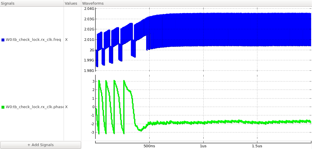
Figure. locking transients of the output clock’s frequency and phase.
tb_meas_bathtub : A testbench for measuring the BER bathtub curve of a CDR
This testbench measures the BER bathtub curve of a CDR by measuring the bit-error rate (BER) of the data sampled with a timing offset from the recovered clock timing. In other words, the output of an extra data sampler triggered by a delayed version of the recovered clock is compared to the output of the main data sampler triggered by the recovered clock to measure the BER and the BER bathtub curve is constructed by plotting the measured BERs versus timing offsets. The statistical simulation capability of XMODEL makes the measurement of BERs as low as 10^-20 possible with ~10,000 samples. From the BER bathtub curve, the maximum timing offset that can be tolerated to achieve a target BER (e.g. 10^-12) can be determined, indicating the timing margin of the CDR.
`include "xmodel.h"

module tb_meas_bathtub();

    parameter real ref_freq = @ref_freq;    // transmitter clock frequency
    parameter real t_offset = @t_offset;    // sampling offset of clock and data recovery
    parameter real t_lock = @t_lock;        // initial simulation time (CDR locking time)
    parameter real RJ_rms = 10e-12;         // transmitter clock RMS jitter in second

    // variables
    xbit    prbs;                           // input prbs stream
    xreal   noise;                          // random noise
    xbit    tx_clk;                         // transmitter clock
    xreal   tx_outp;                        // transmitter output
    xreal   tx_outn;                        // transmitter output
    xreal   chan_outp;                      // channel output
    xreal   chan_outn;                      // channel output
    xreal   rx_inp;                         // receiver input
    xreal   rx_inn;                         // receiver input
    xbit    rx_clk;                         // recovered clock
    xbit    rxclk_w_offset;                 // receiver clock with sampling offset
    xbit    data_ref;                       // recovered data
    xbit    data;                           // recovered data with sampling offset

    // transmitter
    prbs_gen    prbs_gen(.trig(tx_clk), .out(prbs));
    clk_gen     #(.freq(ref_freq), .RJ_rms(10e-12)) clk_tx(tx_clk);
    transition  #(.rise_time(20e-12), .fall_time(20e-12), .value0(-0.1), .value1(0.1))
                tx_driverp(.in(prbs), .out(tx_outp));
    transition  #(.rise_time(20e-12), .fall_time(20e-12), .value0(0.1), .value1(-0.1))
                tx_drivern(.in(prbs), .out(tx_outn));
    // channel
    channel     channelp(.in(tx_outp), .out(chan_outp));
    channel     channeln(.in(tx_outn), .out(chan_outn));

    // noise source
    noise_gen   #(.mean(0.0), .stddev(0.003)) noise_gen(noise);
    add         addp(.out(rx_inp), .in({chan_outp, noise}));
    add			addn(.out(rx_inn), .in({chan_outn, noise}));

    // reference clock and data recovery
    CDR_BangBangPLLCDR   DUT(.in_pos(rx_inp), .in_neg(rx_inn), .data(data_ref), .clk(rx_clk));

    // alexander pd with sampling offset
    bit up, dn;                             // PD output
    delay_xbit  #(.delay(t_offset))
                delay_rxclk(.in(rx_clk),.out(rxclk_w_offset));

    PDD_AlexanderPD alexaner_pd(.in_pos(rx_inp), .in_neg(rx_inn), .up(up), .dn(dn),
                            .data(data), .clk(rxclk_w_offset));

    // probe bit error rate
    probe_ber   #(.start(t_lock))
                probe_ber(.in_ref(data_ref), .in(data), .clk(rx_clk));

endmodule

module channel #(
    parameter real delay = 0.0             // channel transport delay
)(
    input xreal  in,                       // input signal
    output xreal out                       // output signal
);

    filter      #(.gain(0.837), .poles('{3.48e8, 0, 6.61e8, 1.052e9, 6.61e8,-1.052e9,
                6.37e8, 2.387e9, 6.37e8, -2.387e9, 3.584e8, 3.792e9, 3.584e8, -3.792e9}),
                .zeros('{1.821e9, 7.586e8, 1.821e9, -7.586e8, -1.375e9, 2.575e9, -1.375e9,
                -2.575e9, -8.039e8, 4.470e9, -8.039e8, -4.470e9}), .delay(delay))
                channel(.in(in), .out(out));

endmodule
Simulation Results
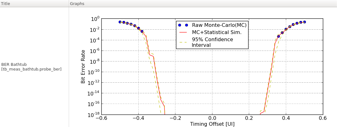
Figure. BER bathtub curve of the CDR.
tb_meas_eyediag : A testbench for measuring the eye diagram of the signal received by a CDR
This testbench measures the eye diagram of the signal received by a CDR, i.e., the transmitter output signal that has propagated through a wireline channel. The XWAVE waveform viewer can plot a statistical eye diagram by folding the signal waveform into a one unit-interval (UI) time range and interpreting the noise information embedded in the signal. A wide eye opening is desirable, where the vertical opening indicates the voltage margin and the horizontal opening indicates the timing margin of the CDR.
`include "xmodel.h"

module tb_meas_eyediag ();
    parameter real ref_freq = 2.0e9;    // transmitter clock frequency
    parameter real RJ_rms = 10e-12;     // transmitter clock RMS jitter in second

    // variables
    xbit    prbs;                       // input prbs stream
    xbit    tx_clk;                     // transmitter clock
    xreal   tx_outp;                    // transmitter output (pos)
    xreal   tx_outn;                    // transmitter output (neg)
    xreal   chan_outp;                  // channel output (pos)
    xreal   chan_outn;                  // channel output (neg)
    xbit    rx_clk;                     // recovered clock
    xbit    data;                       // recovered data
    xreal   noise;                      // random noise
    xreal   noisy_outp;                 // channel output with noise (pos)
    xreal   noisy_outn;                 // channel output with noise (neg)

    // transmitter
    prbs_gen    prbs_gen(.trig(tx_clk), .out(prbs));
    clk_gen     #(.freq(ref_freq), .RJ_rms(RJ_rms)) clk_tx(tx_clk);
    transition  #(.rise_time(20e-12), .fall_time(20e-12), .value0(-0.1), .value1(0.1))
                tx_driver_p(.in(prbs), .out(tx_outp));
    transition  #(.rise_time(20e-12), .fall_time(20e-12), .value0(0.1), .value1(-0.1))
                tx_driver_n(.in(prbs), .out(tx_outn));

    // channel
    channel     channel_p(.in(tx_outp), .out(chan_outp));
    channel     channel_n(.in(tx_outn), .out(chan_outn));

    // noise source
    noise_gen   #(.mean(0.0), .stddev(0.001)) noise_gen(noise);
    add         addp(.in({chan_outp, noise}), .out(noisy_outp));
    add         addn(.in({chan_outn, noise}), .out(noisy_outn));

    // bangbang clock and data recovery
    CDR_BangBangPLLCDR  DUT(.in_pos(noisy_outp), .in_neg(noisy_outn), .data(data), .clk(rx_clk));

    // probing
    probe_xreal #(.start(100e-9)) probe_out(noisy_outp);
    probe_xbit  #(.start(100e-9)) probe_clk(rx_clk);

endmodule

module channel #(
    parameter real delay = 0.0             // channel transport delay
)(
    input xreal  in,                       // input signal
    output xreal out                       // output signal
);

    filter      #(.gain(0.837), .poles('{3.48e8, 0, 6.61e8, 1.052e9, 6.61e8,-1.052e9,
                6.37e8, 2.387e9, 6.37e8, -2.387e9, 3.584e8, 3.792e9, 3.584e8, -3.792e9}),
                .zeros('{1.821e9, 7.586e8, 1.821e9, -7.586e8, -1.375e9, 2.575e9, -1.375e9,
                -2.575e9, -8.039e8, 4.470e9, -8.039e8, -4.470e9}), .delay(delay))
                channel(.in(in), .out(out));

endmodule
Simulation Results
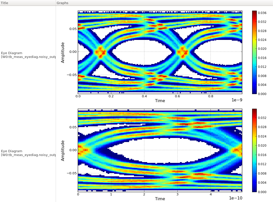
Figure. eye diagram of the CDR.
tb_meas_jhist : A testbench for measuring the jitter histogram of a CDR recovered clock
This testbench measures the jitter histogram of a clock recovered by a clock-and-data recovery unit (CDR). The testbench first waits for the CDR to acquire a lock and then collects the timings of the recovered clock transitions to analyze its jitter histogram. The jitter histrogram shows the probability density function of the CDR clock jitter, which may be influenced by the timing/voltage noise in the input data as well as the noise in the CDR’s internal components.
`include "xmodel.h"

module tb_meas_jhist();

    parameter real ref_freq = 2.0e9;    // transmitter clock frequency
    parameter real RJ_rms = 10e-12;     // transmitter clock RMS random jitter in second
    parameter real t_lock = 2.0e-6;     // CDR locking time

    // variables
    xbit    prbs;                       // input prbs stream
    xbit    tx_clk;                     // transmitter clock
    xreal   tx_outp;                    // transmitter output (pos)
    xreal   tx_outn;                    // transmitter output (neg)
    xreal   chan_outp;                  // channel output (pos)
    xreal   chan_outn;                  // channel output (neg)
    xbit    rx_clk;                     // recovered clock
    xbit    data;                       // recovered data

    // transmitter
    prbs_gen    prbs_gen(.trig(tx_clk), .out(prbs));
    clk_gen     #(.freq(ref_freq), .RJ_rms(RJ_rms))  clk_tx(tx_clk);
    transition  #(.rise_time(20e-12), .fall_time(20e-12), .value0(-0.1), .value1(0.1))
                tx_driver_p(.in(prbs), .out(tx_outp));
    transition  #(.rise_time(20e-12), .fall_time(20e-12), .value0(0.1), .value1(-0.1))
                tx_driver_n(.in(prbs), .out(tx_outn));

    // channel
    channel     channel_p(.in(tx_outp), .out(chan_outp));
    channel     channel_n(.in(tx_outn), .out(chan_outn));

    // bangbang clock and data recovery
    CDR_BangBangPLLCDR   DUT(.in_pos(chan_outp), .in_neg(chan_outn), .data(data), .clk(rx_clk));

    // probing
    probe_xbit  #(.start(t_lock)) probe_clk(rx_clk);

endmodule

module channel #(
    parameter real delay = 0.0             // channel transport delay
)(
    input xreal  in,                       // input signal
    output xreal out                       // output signal
);

    filter      #(.gain(0.837), .poles('{3.48e8, 0, 6.61e8, 1.052e9, 6.61e8,-1.052e9,
                6.37e8, 2.387e9, 6.37e8, -2.387e9, 3.584e8, 3.792e9, 3.584e8, -3.792e9}),
                .zeros('{1.821e9, 7.586e8, 1.821e9, -7.586e8, -1.375e9, 2.575e9, -1.375e9,
                -2.575e9, -8.039e8, 4.470e9, -8.039e8, -4.470e9}), .delay(delay))
                channel(.in(in), .out(out));

endmodule
Simulation Results
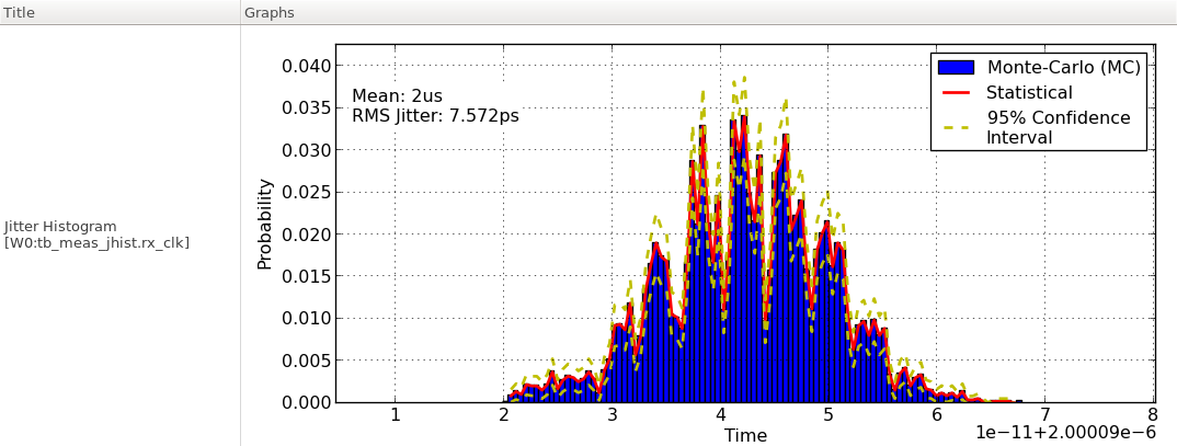
Figure. jitter histogram of the CDR output clock.
tb_meas_jtol : A testbench for measuring the jitter tolerance of a CDR
This testbench measures the jitter tolerance of a CDR by finding the maximum sinusoidal jitter (SJ) that can be tolerated by the CDR while meeting the target BER (e.g. 10^-12). For each SJ frequency, the jtol.py script performs an interactive search to determine the maximum SJ magnitude that can be tolerated. A typical jitter tolerance curve has two regions: a low-frequency region where the jitter tolerance improves as the SJ frequency decreases and a high-frequency region where the jitter tolerance stays relatively constant. The corner frequency between the low- and high-frequency regions indicates the tracking bandwidth of the CDR, while the jitter tolerance in the high-frequency region indicates the timing margin of the CDR.
`include "xmodel.h"

module tb_meas_jtol();

    parameter real ref_freq = @ref_freq;  // transmitter clock frequency
    parameter real SJ_amp = @sj_amp;      // transmitter clock sinusoidal jitter amplitude in UI
    parameter real SJ_freq = @sj_freq;    // transmitter clock sinusoidal jitter frequency in Hz
    parameter real t_lock = @t_lock;      // initial simulation time (CDR locking time)

    // variables
    xbit    prbs;                          // input prbs stream
    xbit    tx_clk;                        // transmitter clock
    xreal   tx_outp;                       // transmitter output (pos)
    xreal   tx_outn;                       // transmitter output (neg)
    xreal   chan_outp;                     // channel output (pos)
    xreal   chan_outn;                     // channel output (neg)
    xbit    rx_clk;                        // recovered clock
    xbit    data;                          // recovered data
    xreal   noise;                         // random noise
    xreal   rx_inp;                        // receiver input (pos)
    xreal   rx_inn;                        // receiver input (neg)

    // transmitter
    prbs_gen    prbs_gen(.trig(tx_clk), .out(prbs));
    clk_gen     #(.freq(ref_freq), .RJ_rms(10e-12), .SJ_amp(SJ_amp), .SJ_freq(SJ_freq))
                clk_tx(tx_clk);
    transition  #(.rise_time(20e-12), .fall_time(20e-12), .value0(0.0), .value1(0.2))
				tx_driver_p(.in(prbs), .out(tx_outp));
    transition  #(.rise_time(20e-12), .fall_time(20e-12), .value0(0.2), .value1(0.0))
				tx_driver_n(.in(prbs), .out(tx_outn));

    // channel
    channel     channel_p(.in(tx_outp), .out(chan_outp));
    channel     channel_n(.in(tx_outn), .out(chan_outn));

    // noise source
    noise_gen   #(.mean(0.0), .stddev(0.003)) noise_gen(noise);
    add         addp(.out(rx_inp), .in({chan_outp, noise}));
    add         addn(.out(rx_inn), .in({chan_outn, noise}));

    // reference clock and data recovery
    CDR_BangBangPLLCDR   DUT(.in_pos(rx_inp), .in_neg(rx_inn), .data(data), .clk(rx_clk));

    // probe bit error rate
    probe_ber   #(.start(t_lock))
                probe_ber(.in_ref(data), .in(data), .clk(rx_clk));

endmodule

module channel #(
    parameter real delay = 0.0             // channel transport delay
)(
    input xreal  in,                       // input signal
    output xreal out                       // output signal
);

    filter      #(.gain(0.837), .poles('{3.48e8, 0, 6.61e8, 1.052e9, 6.61e8,-1.052e9,
                6.37e8, 2.387e9, 6.37e8, -2.387e9, 3.584e8, 3.792e9, 3.584e8, -3.792e9}),
                .zeros('{1.821e9, 7.586e8, 1.821e9, -7.586e8, -1.375e9, 2.575e9, -1.375e9,
                -2.575e9, -8.039e8, 4.470e9, -8.039e8, -4.470e9}), .delay(delay))
                channel(.in(in), .out(out));

endmodule
Simulation Results
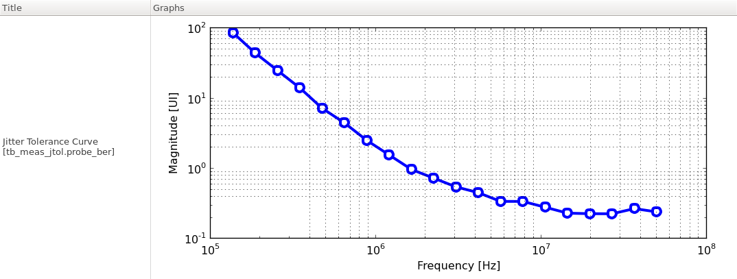
Figure. jitter tolerance of the CDR.
tb_meas_jtran : A testbench for measuring the jitter transfer function of a CDR
This testbench measures the jitter transfer characteristics of a clock-and-data recovery unit (CDR). The testbench measures the jitter transfer function at each frequency by applying a sinusoidal jitter to the input clock using a clk_gen primitive and measuring the magnitude and phase of the resulting sinusoidal response in the recovered clock phase. The jtran.py script repeats this measurement while sweeping the sinusoidal jitter frequency and constructs the overall jitter transfer function of the CDR.
`include "xmodel.h"

module tb_meas_jtran ();

    parameter real ref_freq = @ref_freq;    // transmitter clock frequency
    parameter real SJ_amp = @sj_amp;        // transmitter clock sinusoidal jitter amplitude in UI
    parameter real SJ_freq = @sj_freq;      // transmitter clock sinusoidal jitter frequency in Hz
    parameter real t_lock = @t_lock;        // initial simulation time (CDR locking time)

    // variables
    xbit    prbs;                           // input prbs stream
    xbit    tx_clk;                         // transmitter clock
    xreal   tx_outp;                        // transmitter output (pos)
    xreal   tx_outn;                        // transmitter output (neg)
    xreal   chan_outp;                      // channel output (pos)
    xreal   chan_outn;                      // channel output (neg)
    xbit    rx_clk;                         // recovered clock
    xbit    data;                           // recovered data

    // transmitter
    prbs_gen    prbs_gen(.trig(tx_clk), .out(prbs));
    clk_gen     #(.freq(ref_freq), .SJ_amp(SJ_amp), .SJ_freq(SJ_freq))
                clk_tx(tx_clk);
    transition  #(.rise_time(20e-12), .fall_time(20e-12), .value0(-0.1), .value1(0.1))
                tx_driver_p(.in(prbs), .out(tx_outp));
    transition  #(.rise_time(20e-12), .fall_time(20e-12), .value0(0.1), .value1(-0.1))
                tx_driver_n(.in(prbs), .out(tx_outn));

    // channel
    channel     channel_p(.in(tx_outp), .out(chan_outp));
    channel     channel_n(.in(tx_outn), .out(chan_outn));

    // bangbang clock and data recovery
    CDR_BangBangPLLCDR   DUT(.in_pos(chan_outp), .in_neg(chan_outn), .data(data), .clk(rx_clk));

    // probing
    probe_phase #(.freq(ref_freq), .start(t_lock)) probe_phase(rx_clk);

endmodule

module channel #(
    parameter real delay = 0.0             // channel transport delay
)(
    input xreal  in,                       // input signal
    output xreal out                       // output signal
);

    filter      #(.gain(0.837), .poles('{3.48e8, 0, 6.61e8, 1.052e9, 6.61e8,-1.052e9,
                6.37e8, 2.387e9, 6.37e8, -2.387e9, 3.584e8, 3.792e9, 3.584e8, -3.792e9}),
                .zeros('{1.821e9, 7.586e8, 1.821e9, -7.586e8, -1.375e9, 2.575e9, -1.375e9,
                -2.575e9, -8.039e8, 4.470e9, -8.039e8, -4.470e9}), .delay(delay))
                channel(.in(in), .out(out));

endmodule
Simulation Results
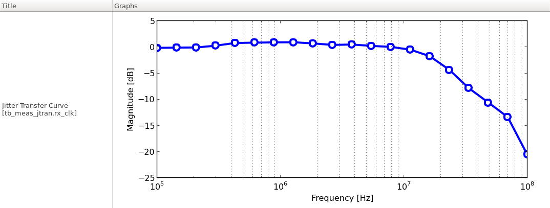
Figure. jitter transfer function of the CDR.