DLL_ChargePumpDLL4DOwithReplica : A multi-phase delay-locked loop (DLL) with a replica loop for wide frequency range operation
A delay locked loop (DLL) is a feedback loop that aligns the phase of an output clock to the phase of an input clock by adjusting the delay of a voltage-controlled delay line (VCDL). To support a wide frequency range of operation without false locks, this DLL employs an replica DLL in addition to the core DLL, which adjusts the delay range of the core VCDL according to the input clock period. In other words, the VCDL has two control voltage inputs, vctrl1 and vctrl2, where vctrl1 is adjusted by the replica DLL and vctrl2 is adjusted by the core DLL. The overall DLL produces multi-phase output clocks by tapping different positions in the delay line.
The core DLL is a type-I charge-pump DLL, and its model is composed of a phase detector (PD), a charge pump (CP), and a voltage-controlled delay line (VCDL). The PD compares the phases of the input and output clocks, clk_in and clk_out, and produces the error expressed as the difference between the up and dn pulse widths. The CP then adjusts the control voltage, vctrl2, so that the delay of the VCDL can align the phases of clk_in and clk_out with a gap of pi radians. When the DLL is in lock, the VCDL produces a set of multiphase clocks clk_out and clk_outb, uniformly spanning the phase range of 0~2*pi.
The replica DLL is another type-I charge-pump DLL, employing a VCDL with a shorter delay than the core VCDL. The shorter delay makes the replica DLL less prone to false lock issues, while its voltage-to-delay characteristic maintains a constant ratio with that of the core VCDL. The replica DLL adjusts the control voltage vctrl1 so that its VCDL delay locks to a fraction of the input clock period. The resulting vctrl1 serves as a coarse-tuning voltage for the core DLL, which adjusts its delay range according to the input clock period.
Ref: Y. Moon, J. Choi, K. Lee, D.-K. Jeong, M. Kim, “An All-Analog Multiphase Delay-Locked Loop Using a Replica Delay Line for Wide-Range Operation and Low-Jitter Performance,” IEEE J. Solid-State Circuits, March 2000.
Input/Output Terminals
| Name | I/O | Type | Description |
| clk_out[3:0] | output | xbit | multi-phase output clocks (pos) |
| clk_outb[3:0] | output | xbit | multi-phase output clocks (neg) |
| clk_in | input | xbit | input clock |
Parameters
| Name | Type | Default | Description |
| Kd1 | real | -12n | VCDL gain for vctrl1 (s/V) |
| Kd2 | real | -6n | VCDL gain for vctrl2 (s/V) |
| vctrl1_0 | real | 0.5 | nominal value for vctrl1 (V) |
| vctrl2_0 | real | 0.5 | nominal value for vctrl2 (V) |
| delay_max | real | 5.6n | maximum limit on VCDL delay (s) |
| delay_min | real | 0.8n | minimum limit on VCDL delay (s) |
| Iup | real | 200u | charge-pump up current (A) |
| Idn | real | 200u | charge-pump down current (A) |
| C | real | 0.8n | loop-filter capacitance (F) |
| delay0 | real | 3.2n | VCDL delay at nominal vctrl values (s) |
| vctrl1_init | real | 0.5 | initial value of vctrl1 (V) |
| vctrl2_init | real | 0.5 | initial value of vctrl2 (V) |
List of Children Cells
| BLK_ChargePumpLoopFilter : A loop filter for charge-pump PLL |
| DLL_ChargePumpDLL4DOwithReplica_ReplicaDLL : A replica delay-locked loop supporting wide-frequency-range operation of a delay-locked loop (DLL) |
| DLN_LinearVCDL4DO2C : A voltage-controlled delay line (VCDL) with dual control inputs, linear V-to-D characteristic, and 4 differential outputs |
| PDC_SRLatchPD : An edge-triggered phase-only detector with an set-reset (SR) latch |
List of Testbenches
| tb_check_lock : A testbench for measuring the locking transient response of a delay-locked loop (DLL) |
| tb_meas_freqstep : A testbench for measuring the frequency step response of a delay-locked loop (DLL) |
| tb_meas_phasestep : A testbench for measuring the phase step response of a delay-locked loop (DLL) |
| tb_meas_tfac : A testbench for measuring the frequency-domain transfer characteristics of a delay-locked loop (DLL) |
tb_check_lock : A testbench for measuring the locking transient response of a delay-locked loop (DLL)
This testbench measures the locking transient of a delay-locked loop (DLL), by initializing the DLL to a condition far from the correct locking point. The phase and delay trajectories ofo the DLL output clock indicate whether the DLL can acquire a correct lock.
When the DLL acquires a correct lock, the difference between the phases of the input clock clk_in and output clock clk_out should converge to a value of pi (rad) and the delay of the VCDL should converge to a half period of the clock.
Simulation Results
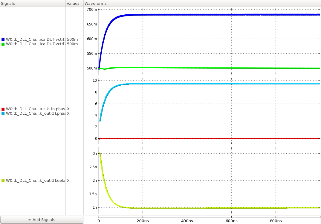
Figure. locking transients of the output clock phase and delay.
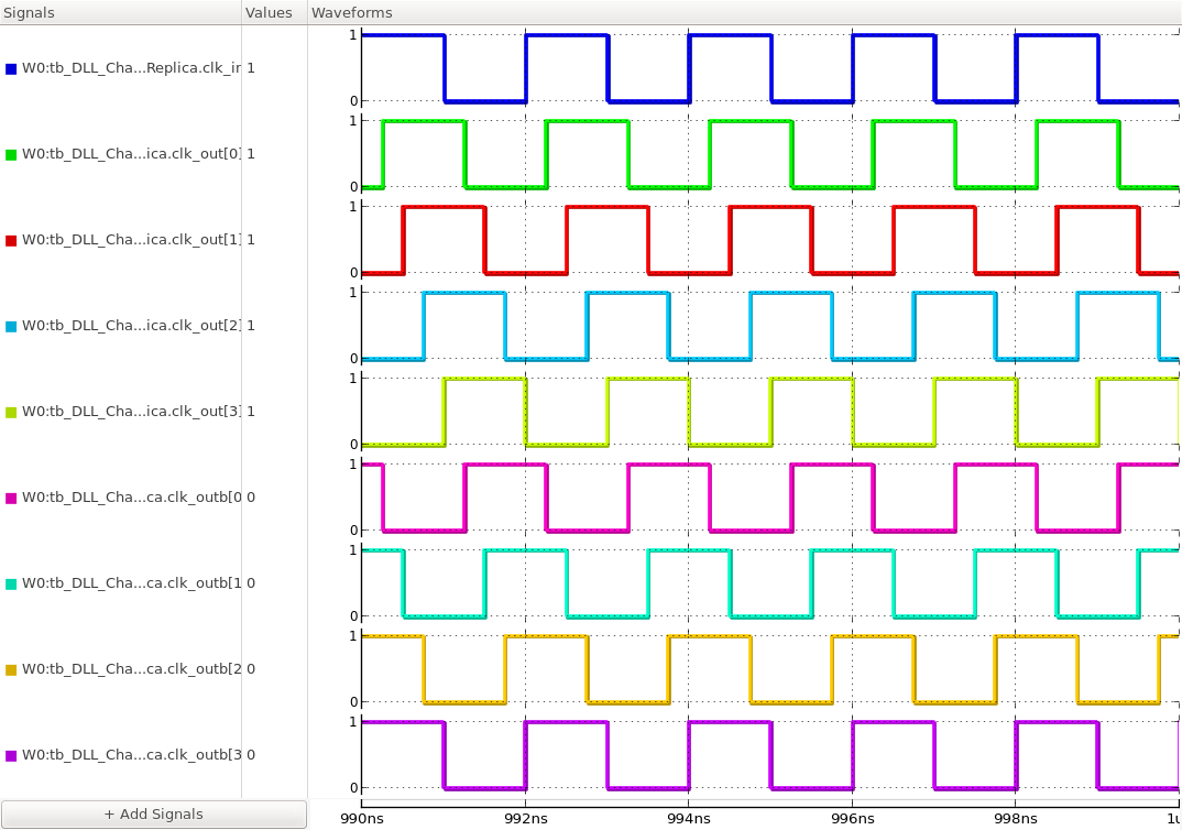
Figure. the input and multiphase output clocks at the locked state.
tb_meas_freqstep : A testbench for measuring the frequency step response of a delay-locked loop (DLL)
This testbench measures the frequency step response of a delay-locked loop (DLL). Once the DLL reaches its lock position, the testbench applies a step change to the frequency of the input clock clk_in using a combination of step_gen and freq_to_clk primitives and observes the response in the frequency of the output clock clk_out[3].
As it is a type-I DLL that locks its delay to a half of the input clock period, the output clock frequency is expected to follow the change in the input clock frequency immediately after the delay while the delay will converge to a half of the new clock period with the settling time determined by the DLL’s bandwidth.
Simulation Results
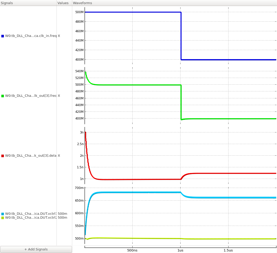
Figure. frequency step response of the VCDL.
tb_meas_phasestep : A testbench for measuring the phase step response of a delay-locked loop (DLL)
This testbench measures the phase step response of a delay-locked loop (DLL). Once the DLL reaches its lock position, the testbench applies a step change in the phase of the input clock clk_in using a combination of step_gen and phase_to_clk primitives and observes the phase response of the output clock clk_out[3].
As it is a type-I DLL that locks its delay to a half of the input clock period, the output clock phase is expected to follow the change in the input clock phase immediately after the delay.
Simulation Results
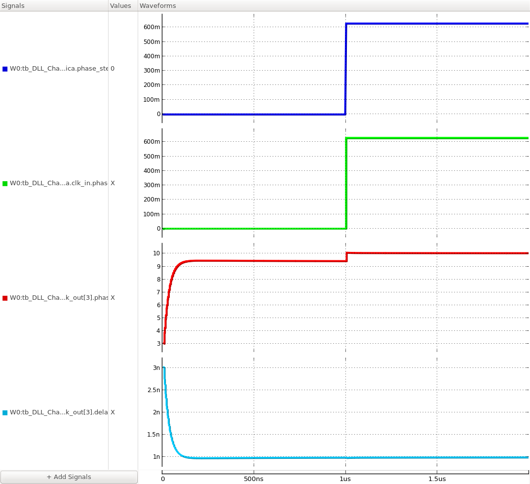
Figure. phase step response of of the VCDL.
tb_meas_tfac : A testbench for measuring the frequency-domain transfer characteristics of a delay-locked loop (DLL)
This testbench measures the frequency-domain transfer characteristics between the input clock period and output delay of a DLL using a probe_ac primitive. The probe_ac primitive supplies an AC stimulus to the input clock period value, with its frequency gradually varying from 100kHz to 100MHz. The primitive also measures the DLL’s output delay as the response and collects the frequency-domain transfer function between the input clock period and output delay.
This input clock period vs. output delay transfer characteristics can indicate the closed-loop bandwidthof a type-I DLL.
Simulation Results
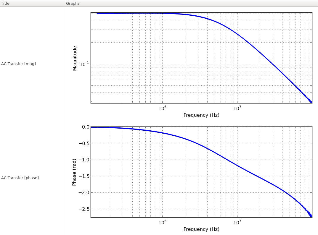
Figure. the frequency-domain transfer characteristics between the input clock period and output delay of the DLL.