DLN_LinearVCDL4DO : A voltage-controlled delay line (VCDL) with a linear V-to-D characteristic and 4 differential outputs
A voltage-controlled delay line (VCDL) controls the delay between the input clock and output clock with a control voltage vctrl. It is typically implemented as a chain of variable delay elements.
This particular VCDL model is a chain of four identical variable delay elements, which collectively produce 4 pairs of complementary clocks clk_out and clk_outb with equal delay spacings. When the total delay through the delay line is equal to a half clock period, the output clocks clk_out and clk_outb become the eight multi-phase clocks that span 360 degrees with uniform phase spacings.
This VCDL model assumes that its delay varies linearly with the control voltage vctrl, that is, delay=delay0+Kvcdl*(vctrl-vctrl0), where the parameter delay0 is the nominal delay of the VCDL when vctrl is at its nominal value defined by the parameter vctrl0 and the parameter Kvcdl is the VCDL gain, i.e., the rate of change in the VCDL delay with respect to the change in vctrl. The delay of the delay line may have the maximum and minimum limits, which are set by the parameters delay_max and delay_min, respectively.
Input/Output Terminals
| Name | I/O | Type | Description |
| clk_out[3:0] | output | xbit | multi-phase output clocks (pos) |
| clk_outb[3:0] | output | xbit | multi-phase output clocks (neg) |
| clk_in | input | xbit | input clock |
| vctrl | input | xreal | control voltage |
Parameters
| Name | Type | Default | Description |
| vctrl0 | real | 0.5 | nominal vctrl value (V) |
| delay0 | real | 3.2n | delay at nominal vctrl value (s) |
| Kvcdl | real | -12n | VCDL gain (s/V) |
| delay_max | real | 5.6n | maximum limit on delay (s) |
| delay_min | real | 0.8n | minimum limit on delay (s) |
List of Children Cells
| BLK_DelayElement : A variable delay element with a linear V-to-D characteristic |
List of Testbenches
| tb_check : A testbench for checking the basic operation of a voltage-controlled delay line (VCDL) |
| tb_meas_tfdc : A testbench for measuring the voltage-to-delay characteristics of a voltage-controlled delay line (VCDL) |
tb_check : A testbench for checking the basic operation of a voltage-controlled delay line (VCDL)
This testbench checks the basic functionality of a voltage-controlled delay line (VCDL). In the first phase, the control voltage vctrl is kept constant at a value that makes the delay between clk_in and clk_out equal to a half period of the input clock clk_in. In this phase, the 8 output clocks clk_out and clk_outb are expected to span 360 degrees uniformly.
And in the second phase, vctrl starts changing and the delay between clk_in and clk_out is expected to change according to the VCDL’s vctrl vs. delay transfer characteristics.
Simulation Results
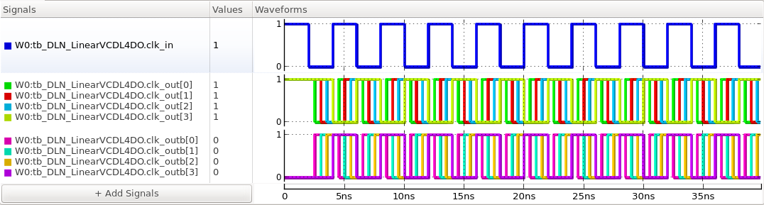
Figure. the delay of the VCDL varying with the change in vctrl.
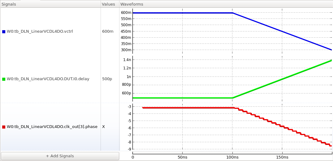
Figure. the input and 8-phase output clocks at the locked state.
tb_meas_tfdc : A testbench for measuring the voltage-to-delay characteristics of a voltage-controlled delay line (VCDL)
This testbench measures the voltage-to-delay characteristics of a voltage-controlled delay line (VCDL), by gradually varying the control voltage vctrl and measuring its delay. The resulting DC transfer characteristics is expected to show the delay changing as the model equation: delay=delay0+Kvcdl*(vctrl-vctrl0).
Simulation Results
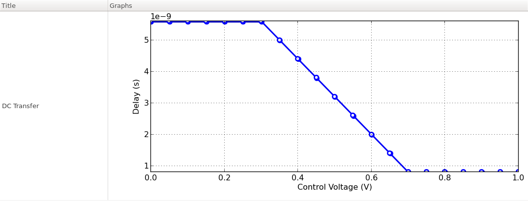
Figure. the voltage-to-delay characteristics of the VCDL.