ADC_SuccApproxADC_Frontend : An analog front-end for a successive approximation register ADC
An analog front-end of a successive approximation register analog-to-digital converter (SAR-ADC) samples an analog input in, generates a reference signal controlled by the digital input sel, and produces the difference between the sampled input and digitally-controlled reference as the analog output out. Typically, this analog front-end of a SAR ADC is implemented as a charge-redistribution digital-to-analog converter (DAC), which can perform sampling, D-to-A conversion, and comparison in one circuit.
This analog front-end model of a SAR-ADC describes a basic charge-redistribution DAC with the circuit primitives, such as capacitor and switch primitives. The model samples the input voltage in at the falling edge of the clock input clk and produces its difference with a reference controlled by the digital value sel.
Input/Output Terminals
| Name | I/O | Type | Description |
| out | output | xreal | the difference between the input and reference |
| clk | input | xbit | sample-and-hold clock |
| in | input | xreal | input voltage |
| sel[5:0] | input | xbit | dac control |
Parameters
| Name | Type | Default | Description |
| vmax | real | 5 | maximum range |
| R | real | 0.01 | sampling resistance |
| C | real | 1e-14 | sampling capacitance |
List of Children Cells
| BLK_Switch1P2T : A single-pole, double-throw switch |
List of Testbenches
| tb_check : A testbench for checking the basic operation of a SAR-ADC analog front-end |
tb_check : A testbench for checking the basic operation of a SAR-ADC analog front-end
This testbench checks the basic operation of a SAR-ADC analog front-end by feeding a zero input and emulating the sequence of the digital input sel assuming the gradually-increasing final output of the SAR-ADC. In other words, when the clock input clk falls, the testbench initializes sel to 6’b000000 and sequentially updates its bits starting from MSB to LSB with the corresponding bits of the final SAR-ADC output target. When clk rises, the testbench sets sel to 6’b111111. After each cycle of clk, the value of target is incremented by 1.
At each rising edge of clk, the SAR-ADC analog front-end is expected to produce the output out with a voltage value equal to the difference between the zero input and the reference controlled by sel, which should increase by a unit step every clk cycle.
`include "xmodel.h"

module tb_check (
    `output_xreal out   // output
);

// signal declarations
xbit        clk;
wire        clk_XMODELCONN0_BIT;
xreal       in;
wire [5:0]  sel;
xbit [5:0]  sel_XMODELCONN0_XBIT;

// connector declarations
xbit_to_bit         xmodel_conn0_clk (.in(clk), .out(clk_XMODELCONN0_BIT));
bit_to_xbit         #(.width(6)) xmodel_conn0_sel (.in(sel[5:0]), .out(sel_XMODELCONN0_XBIT[5:0]));

// instance declarations
ADC_stm_sar_dac     I0 (.clk(clk_XMODELCONN0_BIT), .sel(sel[5:0]));
ADC_SuccApproxADC_Frontend    #(.vmax(5), .R(0.01), .C(1e-14)) DUT (.clk(clk), .sel(sel_XMODELCONN0_XBIT[5:0]), .out(out), .in(in));
dc_gen              #(.value(0.0), .noise(0.0)) XP0 (.out(in));
clk_gen             #(.freq(5e+07), .init_phase(0.0)) XP1 (.out(clk));

// inline dump statements
initial begin
    $xmodel_dumpfile("xmodel.jez");
    $xmodel_dumpvars("level=0");
end

endmodule


module ADC_stm_sar_dac (
    output reg [5:0] sel,
    input clk
);

reg [5:0] target;
int i;

initial target = 0;

always @(clk) begin
    if (clk) #(1ns) sel = 6'b111111;
    else begin
        sel = 6'b000000;
        for (i=5; i>=0; i--) begin
            #(1ns) sel[i] = target[i];
        end
        target += 1;
    end
end

endmodule
Simulation Results
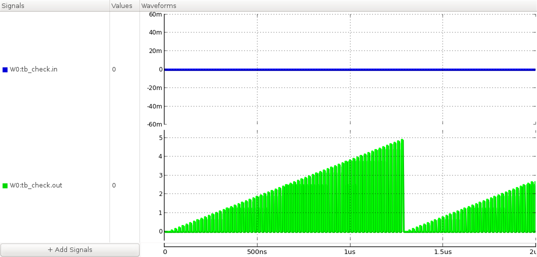
Figure. input and output waveforms.