Languages
Modeling MOSFETs operating in linear/triode region
A MOSFET device operating in a linear region acts as a variable resistor. For example, according to the square-law MOSFET model, the drain current (IDS) of an nMOS transistor with VGS-VTH>0 and sufficiently small VDS follows this approximate equation:
IDS ≅ µnCoxW/L·(VGS-VTH)·VDS = gDS·VDS
where gDS=µnCoxW/L·(VGS-VTH) corresponds to the conductance, or the inverse of the resistance between the drain and source terminals of the transistor. The equation shows that gDS varies with the gate-to-source voltage VGS.
However, I found that the nmosfet and pmosfet primitives of XMODEL do not exhibit the same characteristics. That is, nmosfet or pmosfet primitives modeled with Kp and Vth parameters have a constant gDS equal to Kp×W/L independent of VGS when they are operating in a linear region with VGS-VTH>0 and VDS<VGS-VTH.
I need to model a circuit that relies on this behavior. How do I make the gDS of nmosfet/pmosfet primitives change with the gate-to-source voltage?
The nmosfet and pmosfet primitives of XMODEL model the I-V characteristics of the MOSFET devices using piecewise-linear functions. And you made a correct observation that with only a single pair of Vth and Kp parameters defined, their transconductance (gm) values when operating in the saturation region and the drain-to-source conductance (gDS) when operating in the linear region are both equal to Kp×W/L.
To model a MOSFET device whose gDS changes with VGS, you need to define additional pairs of Vth and Kp values using the Kp_data parameter, and essentially describe the nonlinear I-V characteristics of the device. That is, instead of modeling the transistor with Vth and Kp parameters only:
nmosfet  #(.Vth(0.5), .Kp(1e-3))
         M1 (.d(vd), .g(vg), .s(vs), .b(vb));
model the transistor with multiple pairs of Vth and Kp values using the Kp_data parameter as below:
nmosfet  #(.Kp_data(‘{0.4, 0.5e-3, 0.6, 1.0e-3, 0.8, 1.5e-3, 1.0, 2.0e-3})
         M1 (.d(vd), .g(vg), .s(vs), .b(vb));
Here, the Kp_data parameter defines the transconductance (gm) of the transistor operating in the saturation region as a piecewise-linear function of VGS. For your objective, we recommend listing the 3~5 pairs of VGS and its corresponding gm values uniformly spanning the range of VTH~VDD, where VDD is the nominal supply of the device, or the expected maximum value of VGS. Note that listing more than 5 pairs may adversely impact the simulation speed.
For example, let’s assume a MOSFET device that follows the square-law model. Its drain-to-source conductance (gDS) has the following expression:
gDS = µnCoxW/L·(VGS-VTH).
Let’s assume a case with µnCoxW/L=0.01, VTH=0.5, and VDD=1.0. For the selected VGS values of 0.5, 0.7, 0.9, and 1.1, spanning the range of VTH~VDD, the corresponding gDS values are 0.0, 2e-3, 4e-3, and 6e-3, respectively. Now, list the results as the values of the parameter Kp_data as shown below:
nmosfet  #(.Kp_data(‘{0.5, 2e-3, 0.7, 4e-3, 0.9, 6e-3})
         M2 (.d(vd), .g(vg), .s(vs), .b(vb));
You may have noticed that we listed the values in the sequence of 0.5, gDS(0.7), 0.7, gDS(0.9), 0.9, and gDS(1.1). We will soon confirm that this gives the correct results.
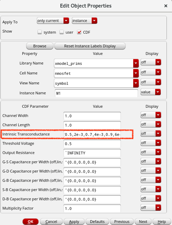
In GLISTER, you can define the Kp_data parameter value of an nmosfet or pmosfet primitive instance by providing a comma-separated list of values to its “Intrinsic Transconductance” parameter, as shown below. This feature is available in the XMODEL 2022.06 or later releases.
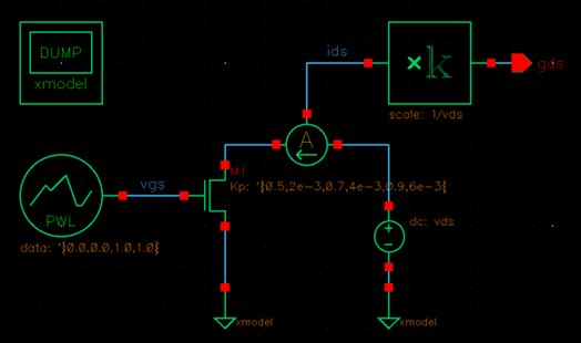
Here is a simple testbench that measures the drain-to-source conductance of an nmosfet primitive instance. The gate-to-source voltage (vgs) is gradually increased from 0.0 to 1.0V while the drain-to-source voltage (vds) is fixed at 0.2V. The drain-to-source conductance (gds) is measured as the drain-to-source current (ids) divided by vds.
Now, here is the simulated waveform, plotting the drain-to-source conductance (gds) versus the gate-to-source voltage (vgs). It confirms that gds indeed increases as a linear function of vgs for vgs≥0.5.
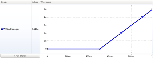
Note that depending on the interval between the VGS values defined in the Kp_data parameter or on the VDS value assumed during the simulation, you may find a different gds versus vgs curve than the one shown above. It is an artifact of the piecewise-linear modeling. Nonetheless, you can still model the drain-to-source conductance of a linear-mode MOSFET device varying with the gate-to-source voltage.
Please login or Register to submit your answer
Linear/triode 영역에서 동작하는 MOSFET 모델링하기
Linear 영역에서 동작하는 MOSFET 소자는 가변저항의 역할을 할 수 있습니다. 예를 들어, square-law MOSFET 모델을 가정하면, nMOS 트랜지스터가 VGS-VTH>0를 만족하고 VDS가 충분히 작을때, 그 드레인 전류 (IDS)는 아래의 근사식을 따릅니다.
IDS ≅ µnCoxW/L·(VGS-VTH)·VDS = gDS·VDS
여기서 gDS=µnCoxW/L·(VGS-VTH)는 트랜지스터의 드레인과 소스 단자 사이의 컨덕턴스 또는 저항값의 역수에 해당합니다. 이 식에서 gDS 값이 게이트-소스 간 전압인 VGS에 따라 변화함을 알 수 있습니다.
그런데, XMODEL의 nmosfet와 pmosfet primitive는 이러한 특성을 따르지 않는 것 같습니다. 즉, nmosfet 또는 pmosfet primitive를 Kp와 Vth 파라메터를 사용해 정의하고, VGS-VTH>0 and VDS<VGS-VTH 전압 조건을 인가하여 linear 영역에서 동작하도록 했을때, 그 드레인-소스 간 컨덕턴스 gDS가 VGS와 무관하게 Kp×W/L 값으로 일정하게 유지되는 것을 관찰하였습니다.
제가 모델하려는 회로는 트랜지스터의 이 특성이 꼭 필요합니다. 어떻게 하면 nmosfet/pmosfet primitive의 gDS 값이 VGS에 따라 변화하도록 모델링할 수 있을까요?
The nmosfet and pmosfet primitives of XMODEL model the I-V characteristics of the MOSFET devices using piecewise-linear functions. And you made a correct observation that with only a single pair of Vth and Kp parameters defined, their transconductance (gm) values when operating in the saturation region and the drain-to-source conductance (gDS) when operating in the linear region are both equal to Kp×W/L.
To model a MOSFET device whose gDS changes with VGS, you need to define additional pairs of Vth and Kp values using the Kp_data parameter, and essentially describe the nonlinear I-V characteristics of the device. That is, instead of modeling the transistor with Vth and Kp parameters only:
nmosfet  #(.Vth(0.5), .Kp(1e-3))
         M1 (.d(vd), .g(vg), .s(vs), .b(vb));
model the transistor with multiple pairs of Vth and Kp values using the Kp_data parameter as below:
nmosfet  #(.Kp_data(‘{0.4, 0.5e-3, 0.6, 1.0e-3, 0.8, 1.5e-3, 1.0, 2.0e-3})
         M1 (.d(vd), .g(vg), .s(vs), .b(vb));
Here, the Kp_data parameter defines the transconductance (gm) of the transistor operating in the saturation region as a piecewise-linear function of VGS. For your objective, we recommend listing the 3~5 pairs of VGS and its corresponding gm values uniformly spanning the range of VTH~VDD, where VDD is the nominal supply of the device, or the expected maximum value of VGS. Note that listing more than 5 pairs may adversely impact the simulation speed.
For example, let’s assume a MOSFET device that follows the square-law model. Its drain-to-source conductance (gDS) has the following expression:
gDS = µnCoxW/L·(VGS-VTH).
Let’s assume a case with µnCoxW/L=0.01, VTH=0.5, and VDD=1.0. For the selected VGS values of 0.5, 0.7, 0.9, and 1.1, spanning the range of VTH~VDD, the corresponding gDS values are 0.0, 2e-3, 4e-3, and 6e-3, respectively. Now, list the results as the values of the parameter Kp_data as shown below:
nmosfet  #(.Kp_data(‘{0.5, 2e-3, 0.7, 4e-3, 0.9, 6e-3})
         M2 (.d(vd), .g(vg), .s(vs), .b(vb));
You may have noticed that we listed the values in the sequence of 0.5, gDS(0.7), 0.7, gDS(0.9), 0.9, and gDS(1.1). We will soon confirm that this gives the correct results.
In GLISTER, you can define the Kp_data parameter value of an nmosfet or pmosfet primitive instance by providing a comma-separated list of values to its “Intrinsic Transconductance” parameter, as shown below. This feature is available in the XMODEL 2022.06 or later releases.
Here is a simple testbench that measures the drain-to-source conductance of an nmosfet primitive instance. The gate-to-source voltage (vgs) is gradually increased from 0.0 to 1.0V while the drain-to-source voltage (vds) is fixed at 0.2V. The drain-to-source conductance (gds) is measured as the drain-to-source current (ids) divided by vds.
Now, here is the simulated waveform, plotting the drain-to-source conductance (gds) versus the gate-to-source voltage (vgs). It confirms that gds indeed increases as a linear function of vgs for vgs≥0.5.
Note that depending on the interval between the VGS values defined in the Kp_data parameter or on the VDS value assumed during the simulation, you may find a different gds versus vgs curve than the one shown above. It is an artifact of the piecewise-linear modeling. Nonetheless, you can still model the drain-to-source conductance of a linear-mode MOSFET device varying with the gate-to-source voltage.
Please login or Register to submit your answer