DLL_ChargePumpDLL8SOwithFLD : A multi-phase delay-locked loop (DLL) with a false-lock detector
A delay locked loop (DLL) is a feedback loop that aligns the phase of an output clock to the phase of an input clock by adjusting the delay of a delay line. This particular DLL employs a false-lock detector to avoid harmonic lock or stuck conditions and produces multiphase output clocks by tapping different positions in the delay line.
This DLL model is composed of a phase detector (PD), a false-lock detector (FLD), a charge pump (CP), and a voltage-controlled delay line (VCDL). The PD compares the phases of the input and output clocks, clk_in and clk_out, and produces the error expressed as the difference between the up and dn pulse widths. The FLD detects whether the DLL is a false lock condition. If it is not, the up and dn signals from the PD are passed to the CP as-is. Otherwise, they are overriden with values that can bring the DLL towards the correct lock. The CP then adjusts the control voltage, vctrl, so that the delay of the VCDL can align the phases of clk_in and clk_out with a gap of 2*pi radians. When the DLL is in lock, the VCDL produces a set of multiphase clocks clk_out, uniformly spanning the phase range of 0~2*pi.
Ref: S. Byun, C.-H. Park, Y. Song, S. Wang, C. S. G. Conroy, B. Kim, “A Low-Power CMOS Bluetooh RF Transceiver with a Digital Offset Cancelling DLL-based GFSK Demodulator,” IEEE J. Solid-State Circuits, October 2003.
Input/Output Terminals
| Name | I/O | Type | Description |
| clk_out[7:0] | output | xbit | multi-phase output clocks |
| clk_in | input | xbit | input clock |
Parameters
| Name | Type | Default | Description |
| Kvcdl | real | -24n | VCDL gain (s/V) |
| vctrl0 | real | 0.5 | nominal vctrl value (V) |
| delay0 | real | 5.6n | VCDL delay at nominal vctrl value (s) |
| delay_max | real | 11.2n | maximum limit on VCDL delay (s) |
| delay_min | real | 1.6n | minimum limit on VCDL delay (s) |
| vinit | real | 0.5 | initial vctrl value (V) |
| Iup | real | 400e-06 | charge-pump up current (A) |
| Idn | real | 400e-06 | charge-pump down current (A) |
| C | real | 0.4n | loop-filter capacitance (F) |
List of Children Cells
| BLK_ChargePumpLoopFilter : A loop filter for charge-pump PLL |
| DLL_ChargePumpDLL8SOwithFLD_FalseLockDetector : A false-lock detector (FLD) for a multi-phase delay-locked loop (DLL) |
| DLN_LinearVCDL8SO : A voltage-controlled delay line (VCDL) with a linear V-to-D characteristic, 8 single-ended outputs |
| PDC_SidiropoulosPD : A precharge-type phase-only detector by S. Sidiropoulos |
List of Testbenches
| tb_check_lock : A testbench for measuring the locking transient response of a delay-locked loop (DLL) |
| tb_meas_freqstep : A testbench for measuring the frequency step response of a delay-locked loop (DLL) |
| tb_meas_phasestep : A testbench for measuring the phase step response of a delay-locked loop (DLL) |
| tb_meas_tfac : A testbench for measuring the frequency-domain transfer characteristics of a delay-locked loop (DLL) |
tb_check_lock : A testbench for measuring the locking transient response of a delay-locked loop (DLL)
This testbench checks the locking transient of a delay-locked loop (DLL), by initializing the DLL to a condition far from the correct locking point. The phase and delay trajectories of the DLL output clock indicate whether the DLL can acquire a correct lock.
When the DLL acquires a correct lock, the difference between the phases of the input clock clk_in and output clock clk_out should converge to a value of 2*pi (rad) and the delay of the VCDL should converge to one period of the clock.
Simulation Results
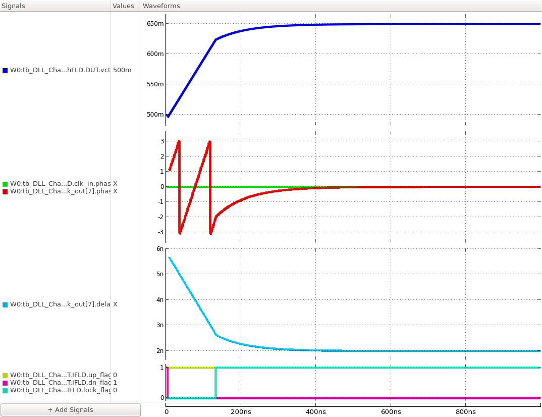
Figure. locking transients of the output clock phase and delay.
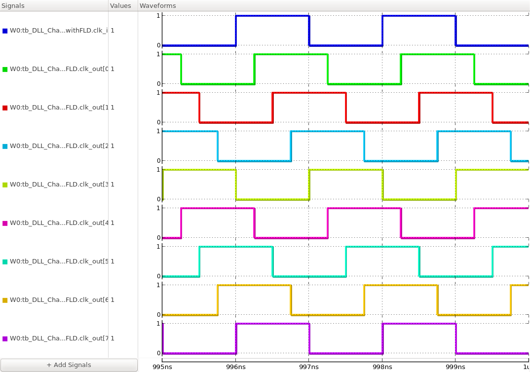
Figure. the input and multiphase output clocks at the locked state.
tb_meas_freqstep : A testbench for measuring the frequency step response of a delay-locked loop (DLL)
This testbench measures the frequency step response of a delay-locked loop (DLL). Once the DLL reaches its lock position, the testbench applies a step change to the frequency of the input clock clk_in using a combination of step_gen and freq_to_clk primitives and observes the response in the frequency of the output clock clk_out[7].
As it is a type-I DLL that locks its delay to one input clock period, the output clock frequency is expected to follow the change in the input clock frequency immediately after the delay while the delay will converge to the new clock period with the settling time determined by the DLL’s bandwidth.
In particular, to check the functionality of the false-lock detector (FLD), the step change applied to the input clock frequency is made large enough to cause a stuck condition. In this case, the FLD is expected to assert up_flag or dn_flag and forces the DLL towards the correct lock. When the DLL approaches near the correct lock position, the FLD is expected to de-assert up_flag and dn_flag and assert lock_flag instead.
Simulation Results
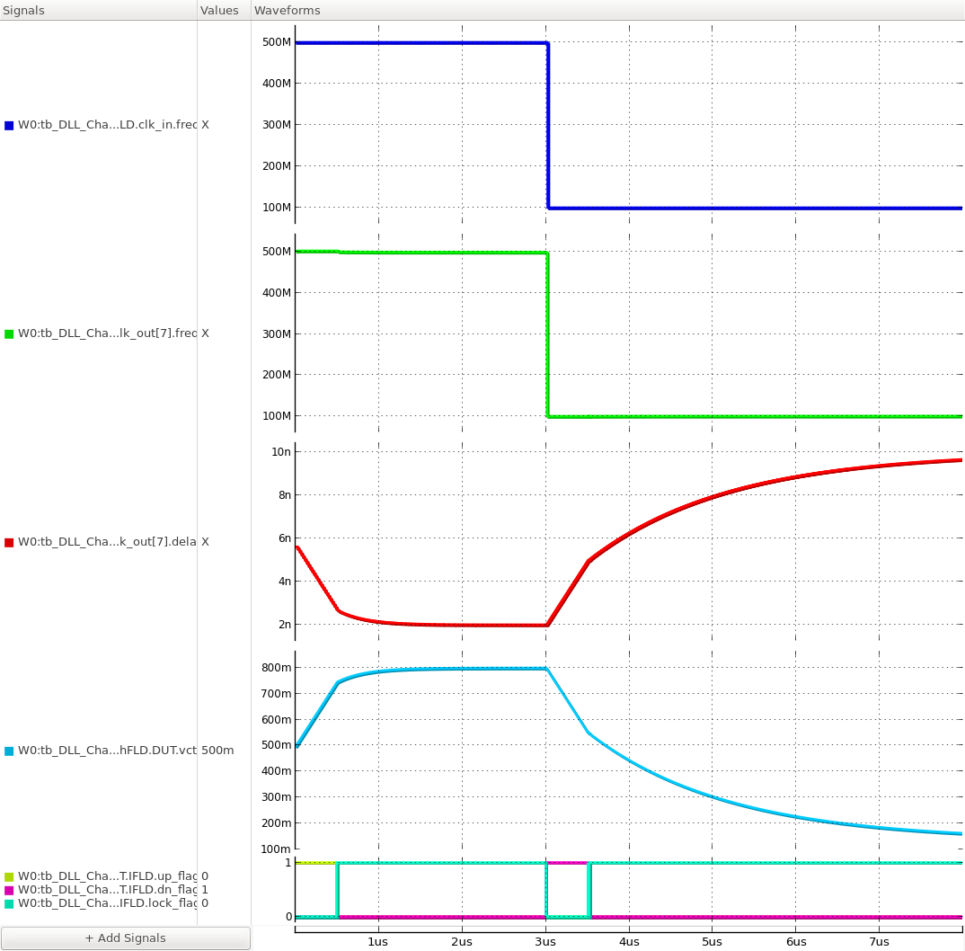
Figure. frequency step response of the DLL.
tb_meas_phasestep : A testbench for measuring the phase step response of a delay-locked loop (DLL)
This testbench measures the phase step response of a delay-locked loop (DLL). Once the DLL reaches its lock position, the testbench applies a step change in the phase of the input clock clk_in using a combination of step_gen and phase_to_clk primitives and observes the phase response of the output clock clk_out[7].
As it is a type-I DLL that locks its delay to the input clock period, the output clock phase is expected to follow the change in the input clock phase immediately after the delay.
Simulation Results
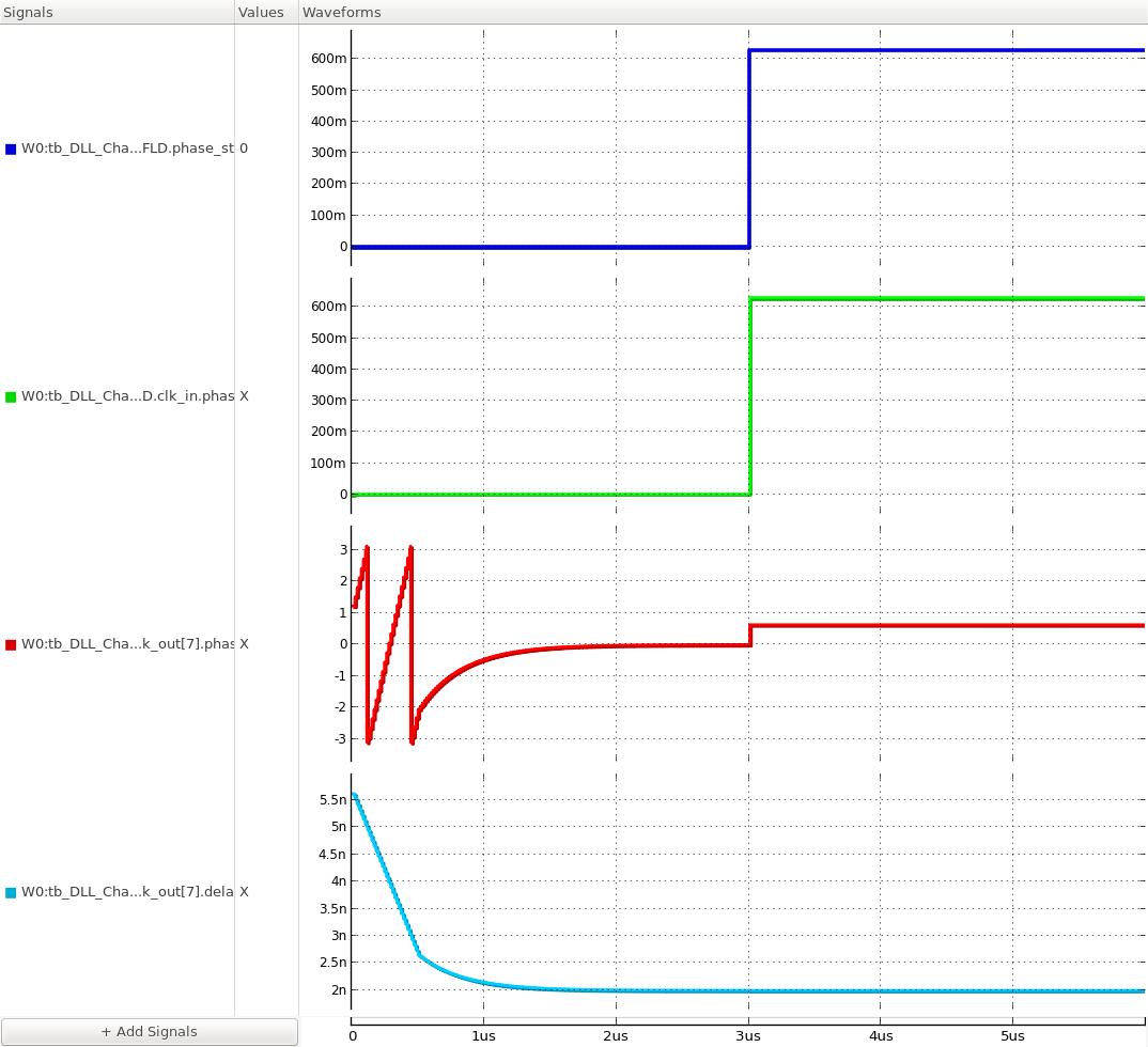
Figure. phase step response of the VCDL.
tb_meas_tfac : A testbench for measuring the frequency-domain transfer characteristics of a delay-locked loop (DLL)
This testbench measures the frequency-domain transfer characteristics between the input clock period and output delay of a DLL using a probe_ac primitive. The probe_ac primitive supplies an AC stimulus to the input clock period value, with its frequency gradually varying from 20kHz to 20MHz. The primitive then measures the DLL’s output delay as the response and collects the frequency-domain transfer function between the input clock period and output delay.
This input clock period vs. output delay transfer characteristics can indicate the closed-loop bandwidth of a type-I DLL.
Simulation Results
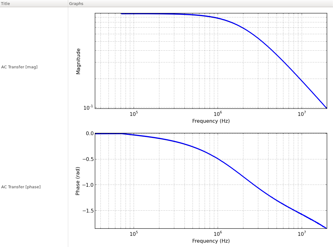
Figure. the frequency-domain transfer characteristics between the input clock period and output delay of the DLL.